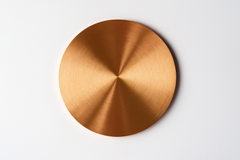
Cell Lab 4N5 (99.995%) Copper (Cu) Sputtering Target
High-Conductivity Copper Target for Thin Film Deposition and Electronic Applications
General Description
Cell Lab 4N5 (99.995%) Copper Sputtering Target is a high-purity metallic target engineered for semiconductor, microelectronic, and optical thin-film applications. Copper is a reddish-orange, ductile, and malleable transition metal known for its exceptional electrical and thermal conductivity.
In sputtering processes, it is widely used to deposit conductive layers, seed films, and reflective coatings across various industries including MEMS fabrication, data storage, and advanced circuitry.
Key Features
-
Ultra-High Purity (99.995%) – Reduces oxygen and sulfur contamination, ensuring consistent conductivity.
-
Excellent Conductive Properties – Ideal for electrodes, interconnects, and transparent conductive coatings.
-
Superior Film Adhesion – Ensures dense, uniform, and highly conductive thin films.
-
Versatile Sputtering Compatibility – Suitable for DC, RF, and magnetron sputtering systems.
-
Customisable Options – Dimensions, bonding types, and purity grades (4N–5N) available upon request.
Technical Specifications
| Parameter | Specification |
|---|---|
| Material Type | Copper |
| Symbol | Cu |
| Atomic Number | 29 |
| Atomic Weight | 63.546 |
| Density | 8.96 g/cm³ |
| Melting Point | 1,083 °C |
| Boiling Point | 2,567 °C |
| Crystal Structure | Cubic |
| Colour/Appearance | Red/Orange, Metallic |
| Purity | 99.99%, 99.995% |
| Thermal Conductivity | 400 W/m·K |
| Coefficient of Thermal Expansion | 16.5 × 10⁻⁶ /K |
| Sputtering Method | DC or Magnetron |
Applications & Industries
-
Microelectronics – Conductive interconnects, integrated circuits, and seed layers.
-
Photovoltaics – Back electrodes and contact layers in thin-film solar cells.
-
Optics – Reflective and decorative coatings with excellent adhesion.
-
Data Storage – Thin conductive layers for HDDs and magnetic components.
-
Aerospace & Defence – Corrosion-resistant conductive coatings for components.
FAQ
Q1: Can copper targets be used in reactive sputtering environments?
Yes, but inert gas environments (Ar) are preferred to maintain purity and prevent oxide formation.
Q2: What bonding options are available?
Cell Lab offers indium-bonded copper backing plates for improved thermal management.
Q3: Is the 5N purity necessary for all applications?
For high-performance electronics and semiconductor coatings, 5N purity ensures minimal contamination and superior conductivity.
Q4: Are custom dimensions available?
Yes. We provide custom diameters, thicknesses, and shapes for compatibility with all major sputtering systems.


